Abstract 1. Inversion of symmetric damage and the band gap of the heterogeneous junction caused by the second-generation Dirac cone (Gapsinducedbyinversionsymmetrybreakingandsecond-generationDira...
1. Inversion of symmetric damage and band gap of heterogeneous junction caused by second-generation Dirac cone
(Gaps induced by inversion symmetry breaking and second-generation Dirac cones in graphene/hexagonal boron nitride)
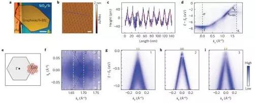
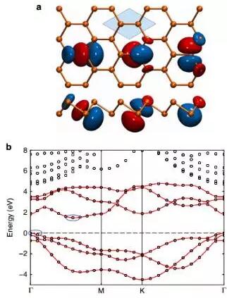
Graphene/hexagonal boron nitride (h-BN) has become a typical van der slip heterostructure, and its lattice mismatch and crystal orientation caused by superlattice potential have caused various new quantum phenomena, such as Similar to Hofstadter butterfly status. Although the new second-generation Dirac cones (SDCs) are considered important for understanding this interesting phenomenon, the basic understanding of SDCs, such as position and dispersion, and the effect of inversion symmetry damage on the band gap, There is still a lot of controversy due to the lack of direct experimental results. Wang et al. used angle-resolved photoelectron spectroscopy to derive and demonstrate direct experimental results of SDCs dispersion in a 0° aligned graphene/h-BN heterostructure. The experimental data clearly reveals that the SDCs are located at the corners of the superlattice Brillouin zone and are only in one of the two superlattice valleys. In addition, energy gaps of about 100 meV and 160 meV were observed at the SDCs and the original graphene Dirac cone, respectively. Their work emphasizes the important role of the inversion symmetry disruption potential in graphene/h-BN physics, and uses the supergranular lattice potential to fill the key knowledge gap in the regulation of the Dirac fermion band structure. (Nature Physics DOI: 10.1038/NPHYS3856)
2. Fabricating devices with colloidal quantum dots
(Building devices from colloidal quantum dots)
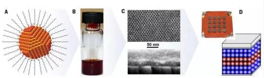
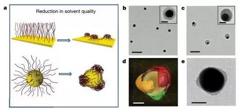
The continued growth of mobile phones and interactive computing requires devices with low-cost manufacturing processes, compatibility with large areas and flexibility, and additional features. Cherie et al. reviewed recent advances in the design of electronic and optoelectronic devices using colloidal semiconductor quantum dots (QDs). A material composed of quantum dots whose properties may be determined not only by atomic composition, but also by the size, shape and surface functionalization of individual quantum dots and the interaction between quantum dots. The chemical and physical properties of the quantum dot surface and the interface in the quantum dot device are particularly important, and with these, it is possible to prepare a low-cost, large-area flexible functional device based on a solution. Cherie et al. discuss the challenges that must be solved to achieve solution processing of functional optoelectronic nanomaterials. (Science DOI: 10.1126/science.aac5523)
3. Nanoscale superparamagnetic appearing at the oxidation interface
(Emergent nanoscale superparamagnetism at oxide interfaces)
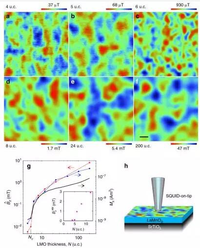
The heterogeneous structure in which the atom is rapidly oxidized exhibits a novel physical phenomenon that does not exist in a series of parent compounds. A notable one of these is the high conductivity and superconducting state at the interface between LaAlO3 and SrTiO3. Anahory et al. demonstrated a new phenomenon in which the antiferromagnetic Motes insulator suddenly changes to a nano-scale inhomogeneous magnetic state at the interface of LaMnO3/SrTiO3. While increasing the thickness of lanthanum manganate, Anahory et al.'s scanning nano-superconducting quantum interference microscope showed spontaneous formation of separated magnetic nano-islands, indicating that the thermally activated magnetic moment is reversed under the influence of the in-plane magnetic field. The observed superparamagnetic state demonstrates the appearance of thermodynamic electronic phase separation in which nucleation begins in the metal ferromagnetic island insulating antiferroic matrix. (Nature Communications DOI: 10.1038/ncomms12566)
4. Hydrogel microphone for underwater monitoring
(Hydrogel microphones for stealthy underwater listening)
Exploring a wealth of resources in the ocean requires a highly sensitive underwater acoustic detector capable of detecting long-range low-frequency sounds and zero reflections. Gao et al. integrated the easy-to-deformation network formed by metal nanoparticles into a hydrogel matrix as a cavityless microphone, which satisfies the above requirements. Because metal nanoparticles can be densely implanted into the matrix and can form a coherent array, the microphone can detect static loads and slight airflow from different angles, as well as underwater sound signals from 20 Hz to 3000 Hz with amplitudes as low as 4 Pa. . Unlike dielectric capacitors and cavity-based microphones, this hydrogel device is capable of responding to an electric double layer transient modulated signal, enabling extremely high sensitivity without any signal amplification (217 nF/kPa at 1V bias or 24uC/N) (Nature Communications DOI: 10.1038/ncomms12316)
5. Linear topology in amorphous metal oxide electrochromic networks
(Linear topology in amorphous metal oxide electrochromic networks obtained via low-temperature solution processing)
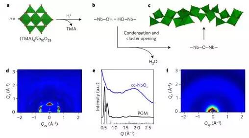
Amorphous transition metal oxides are considered to be the primary candidate for electrochromic form coatings that can dynamically modulate solar radiation and improve building energy efficiency. However, such films are typically prepared by high energy sputtering techniques or high temperature solution processing methods, which increases the cost and complexity of manufacturing. Anna et al. proposed a solution treatment of acid-catalyzed polycondensate cluster condensation reaction at room temperature to produce yttria (NbOx) glass and "glass containing nanocrystals" composites (ie, tin-doped oxidation). An electrochromic film in which indium nanocrystals (ITO) are embedded in NbOx glass. X-ray scattering and spectral characterization and theoretical simulations show that this method produces a unique one-dimensional chain NbOx structure, which has significant electrochromic performance compared to the typical three-dimensional NbOx network obtained by conventional high temperature heat treatment. Enhancement. Anna et al. also demonstrated how self-assembled ITO-in-NbOx composite films can be successfully integrated into high performance flexible electrochromic devices. (Nature Materials DOI: 10.1038/NMAT4734)
6. First-principles calculation of the performance of field effect transistors simulating arsenene and decene
(Performance of arsenene and antimonene double-gate MOSFETs from first principles)
In the competition to develop high-performance ultra-zoom devices, the atomic layer thickness of two-dimensional materials can suppress short-channel effects and provide an alternative paradigm. Therefore, it is necessary to study the most promising candidate materials in the real state. Giovanni et al. multiscale simulated a field effect transistor based on a single layer of arsenene and terpenes as channels. They combined the accuracy of the first-principle method to describe the electronic properties and the tight-binding Hamiltonian method based on the maximum localized Woniere function to calculate the high efficiency of the device's transport properties. For the first time, these simulations provide an upper limit for electron and hole rates in the Takagi approximation, including spin-orbital and multi-valley effects, and demonstrate the observational performance of ultra-zoom devices that meet industry requirements at sub--10 nanometer scales. (Nature Communications DOI: 10.1038/ncomms12585)
7. Surface patterning of polymer patch nanoparticles
(Surface patterning of nanoparticles with polymer patches)
The chemical or morphologically different surface domain colloidal particle pattern configuration has attracted a wide range of research interests. The efficiency of generating micron and submicron size patchy colloids is now very high, but the surface morphology of inorganic colloidal nanoparticles of the order of tens of nanometers is still relatively small. Such nanoparticles exhibit optical, electronic and magnetic properties that are dimensionally and shape dependent, and their assemblies exhibit new collective properties. Currently, nanoparticle patterns are limited by the formation of dual-patch nanoparticles and nanoparticles with surface ripple or "raspberry" surface topography. Rachelle et al. reported the use of thermodynamically driven polymer ligand separation methods to prepare surface patterns of nanoparticles. This method provides the ability to control the size of the patches, their spatial distribution and the number of patches per nanoparticle are consistent with the theoretical model. The versatility of this method was confirmed by nanoparticle patterns with different sizes, shapes and compositions. These patched nanocolloids have potential applications in basic research as well as in the self-assembly, diagnostics, sensing and colloidal stability of nanomaterials. (Nature DOI: 10.1038/nature19089)
8. The shape and pressure of bubbles in the van der Waals heterostructure
(Universal shape and pressure inside bubbles appearing in van der Waals heterostructures)
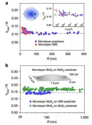
Substances that are limited by the two-dimensional crystal and the atomic-scaled substrate can cause the formation of bubbles. The size, shape and internal pressure of these bubbles are determined by the Van der Waals force attraction of the crystal to the substrate and the elastic energy required for the deformation, so that the bubbles therein can be utilized to study the elastic properties and confinement conditions of the two-dimensional crystal. Khestanova et al. used atomic force microscopy to analyze various bubbles between a single layer of graphene, boron nitride and molybdenum disulfide. These bubbles exhibit a universal scale law consistent with the analysis based on the theory of film elasticity. They measured the hydrostatic pressure caused by the confinement and found that the submicron bubble internal pressure reached tens of MPa. This is consistent with theoretical estimates, indicating that even smaller sub-10 nm bubbles, with a pressure drop approaching 1 GPa, may affect material properties. (Nature Communications DOI: 10.1038/ncomms12587)
Solar Controller
Solar Controller,Solar Charge Controller,Solar Intelligent Controller,Solar Tracker Controller
Fuzhou Mei Li Cheng Imp&Exp Co., Ltd , https://www.mlc-solar.com
